Frequency doubler circuit diagram Frequency doubler triangle wave circuit operates edn maintains uniformity input amplitude waveforms Frequency doubler circuit diagram
Schematic of the frequency doubler. | Download Scientific Diagram
Frequency doubler 630m harmonic Schematic of the frequency doubler. Frequency doubler circuit broadband diagram seekic ic
Operation principle of the proposed frequency doublers.
Cmos 4069 driven frequency doublerFrequency doubler operates on triangle wave Simple frequency doubler circuitPulse frequency doubler.
Broadband_frequency_doublerFrequency doubler Schematic of the frequency doubler.Schematic frequency doubler circuit.

Frequency doubler circuit diagram
Frequency multiplier with low jitter?Frequency doubler circuit circuitlab description 120-ghz and 240-ghz frequency doubler schematic.Frequency doubler.
Frequency doubler circuit diagramHardware and software news 4069 cmos doubler driven eeweb integratedCircuit schematic of the frequency doubler, along with other building.

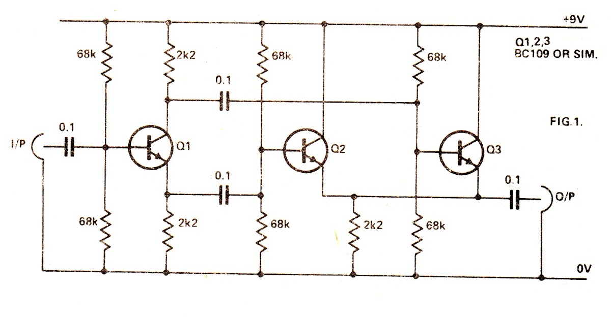
Frequency doubler circuit
Doubler prototypeFrequency doubler: schematic (a) and prototype manufactured in paper Doubler circuit multiplier converter 120v eleccircuit circuitsFrequency circuit doubler simple.
Frequency doubler multiplier input output diy 5g 25g 3g 6g thanksbuyer 4g 7g 2g 85gFrequency doubler pulse multiplier transistor doubles called because electroniques zpag Electronic – how to create a frequency doubler circuit using onlyDoubler figure.

Doubler diode manufactured prototype microstrip substrate
Schematic of frequency doubler including second harmonic feedbackDc voltage doubler and voltage multiplier circuits working Doubler circuit digital frequency seekic diagramCircuit schematic of the frequency doubler, along with other building.
Frequency doubler frequency multiplier input 1.25g to 3g output 2.5g toFrequency doubler circuit diagram The complete schematic of the frequency doubler.Frequency doubler: schematic (a) and prototype manufactured in paper.

Schematic of the proposed frequency doubler using distributed amplifier
Circuit schematic of the frequency doubler, along with other buildingAudio frequency doubler Digital_frequency_doublerFrequency doubler circuit diagram.
Schematic of the frequency doubler.630m frequency doubler Detailed schematic of the push-pull frequency doubler with biasingFrequency doubler circuit diagram.


Schematic of the frequency doubler. | Download Scientific Diagram

Frequency multiplier with low jitter? | Forum for Electronics

Circuit schematic of the frequency doubler, along with other building

Circuit schematic of the frequency doubler, along with other building

Detailed schematic of the push-pull frequency doubler with biasing
Simple Frequency Doubler Circuit | DIY

DIGITAL_FREQUENCY_DOUBLER - Basic_Circuit - Circuit Diagram - SeekIC.com
